


Cleanroom News, Cleanroom Technology
How 2D Graphene Exists in a 3D World

Jul
Flatland: A Romance in Many Dimensions is a novella exploring the world through the eyes of ‘A Square,’ a character who exists in only two dimensions. A Square lives in Flatland, a world conceptualized by writer Edwin A. Abbott in 1884 as a critical commentary upon the hierarchical nature of the rigidly stratified society of Victorian England. In the book, male characters are depicted as polygons, their social worth and prestige deriving from their number of sides. Female characters are reduced to simple lines and are forced to announce their presence in public by sounding a ‘peace cry’ to ensure that others, who in a head-on meeting would perceive them only as points, are alerted to their danger. In depicting the lives of the 2D characters, Abbott sought to highlight the inequity in roles of women in nineteenth century Britain and also the constraints of class-based stricture in the lives of men. While it received little critical acclaim at the time of writing, interest in the novella was revived following Einstein’s publication of his General Theory of Relativity, which saw the first positing of a fourth dimension, and in more contemporary times theoretical physicists Carl Sagan and Stephen Hawking have both commented on the literary thought experiment.
So what does a crazy fantasy tale about imaginary 2D characters have to do with modern physics and the cleanroom?
Everything, if researchers at the United Kingdom’s University of Manchester have their way. Nestled inside some very real three-dimensional contamination controlled environments, exotic and innovative 2D materials are being spun from a very commonplace element: graphite. And these materials have the power to revolutionize the creation of products as diverse as fuel cells, spinal cord scaffolds, and aircraft chassis. Let’s take a closer look….
In 2004, professors at the University of Manchester in the north-west of England were cleaning a piece of graphite stone.
Ripping off a strip of sellotape – aka Scotch tape – they pressed it to the stone and noticed that it removed a micro-thin layer of graphite.
By folding it in the sticky tape over and over, thinning the material with each iteration, the researchers were able to whittle it down to a layer of a single atom in thickness. Expected to be fragile, the one atom thick crystals were found to be strong and light, hard as diamond and more conductive than copper. Graphene was born.(1)
Aware that their discovery could be the key to revolutionizing myriad industries – from fuel cell production to aviation – the team submitted their research to the eminent journal Nature. From which it was rejected not once but twice. According to an article in the New Yorker, ‘one reader stated that isolating a stable, two-dimensional material was “impossible,” and another said that it was not “a sufficient scientific advance.”’(2) Despite this initial ignominy, a later paper in the journal Science, ‘Electric Field Effect in Atomically Thin Carbon Films’, drew rave reviews, with the EVP of Samsung Advanced Institute of Technology, Youngjoon Gil, commenting ‘“It was as if science fiction had become reality.”’(3) The researchers, Professor Andre Geim and then Ph.D. student Kostya Novoselov, ultimately went on to win the Nobel Prize for Physics in 2010, becoming the university’s 24th and 25th Nobel Laureates and, in 2013, were recognized as Freemen of the City of Manchester. A rare accolade indeed.
But what is graphene and why is it such a cause for excitement?
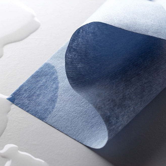
In essence, the super-skinny layer of graphite is a rising star in the world of materials science and condensed-matter physics. It has a specific surface area of 2630m2/g which compares favorably against carbon nanotubes at 100 to 1000 m2/g and is similar to that of activated carbon. Indeed it is an allotrope of carbon and is structured on the atomic level in a hexagonal lattice which goes some way to accounting for its strength and flexibility – strength which is 300 times that of steel in a material that is simultaneously lighter than air and harder than diamond. And, in case you missed it, this nanomaterial is two-dimensional. Let’s just pause to consider that for a moment. It is a material in our physical 3D world but it lacks a dimension. In fact, it is the first 2D crystal ever known.
Moreover if that’s not enough to enter it into any putative Physics Hall of Fame, graphene also gave rise to new paths into the study of low-dimension physics and a cornucopia of additional single atom thickness materials that exist in the 2D space, materials known collectively as transition-metal dichalcogenides (TMDCs). TMDCs are created by pairing one atom of transition metal with two of chalcogen. Transition metal elements include zirconium (Zr), molybdenum (Mo), palladium (Pd), and vanadium (V), amongst 8 others, and create materials such as molybdenum disulphide (MoS2). So do these additional materials have an advantage over the ‘original and best’ graphene? In some ways, they do. Graphene inherently has super-effective electrical and thermal conductivity – approximately 1000 times that of copper. But it lacks a ‘band gap’ – the difference in electron volts between the top of the valence band and the bottom of the conduction band. This ‘gap’ facilitates the manipulation of a material’s conductivity – allowing it to be ‘on’ or ‘off,’ statuses that – in semiconductor terms – equate to ‘1’ or ‘0’. But graphene, a hard-working material, is conductive all the time.
But outside of semiconductors, graphene – a transparent product that absorbs only 2% of the light passing through it – seems to have a promising future. According to Robert Friedel, University of Maryland’s technology historian, ‘The more innovative – the more breaking-the-mold – the innovation is, the less likely we are to figure out what it is really going to be used for.’ But this may not be axiomatic for graphene – let’s hop back across the Pond to Britain to see why…

According to a March 2017 article in the business section of The Telegraph, airline entrepreneur Sir Richard Branson is utterly beguiled by graphene. As a former champion of carbon fiber in aircraft construction, Branson has long battled the base cost of fuel burn in aviation. His mission, when encouraging both Boeing and Airbus to incorporate carbon fiber as opposed to aluminum, was to create ‘massively lighter […] planes, which […] would make a difference on fuel burn.’(4) And given that Branson owns a 51% stake in the carrier Virgin Atlantic which is forecasting a loss this year due to a 50% increase in fuel costs, this is clearly close to his heart and his financial bottom line.
So let’s assume that Branson is correct in wagering that graphene is the key to bringing down the spiraling costs of travel – but what else can it do? How about improve fuel cell technology? In research conducted at the Italian Institute of Technology (IIT), based in Genova, Italy, the next generation of lithium-ion cells use graphene for the battery’s anode.(5) The material was isolated by breaking up a solution of graphite particles using ultrasound, with centrifugal force separating out the graphene particles from the mix.
The liquid graphene is then painted onto the battery’s copper surfaces, increasing its conductivity and raising the overall performance by 25%.
Moreover, the research team is so impressed by this application that it recently showcased a variety of new products and developments at the Mobile World Congress 2017. Held in Barcelona, Spain, the Congress was attended by more than 100,000 people from 208 countries.(6) And many of them were keen to visit the Graphene Experience Zone in which IIT’s graphene helmet, supercapacitor, and electrodes for prosthetic hands were on display.(7)
Back on this side of the Pond, at Massachusetts Institute of Technology (MIT) researchers are experimenting with transforming 2D graphene into 3D objects using additive manufacturing which allows products to be 10 times stronger than steel while still maintaining their weight advantage. In a January 2017 interview with ComputerWorld, MIT’s Markus Buehler of the Department of Civil and Environmental Engineering (CEE) explained that researchers had created ‘new graphene structures using a proprietary, multi-material 3D printer; the structures [having] a “sponge-like” configuration.’(8) As Zhao Qin, McAfee Professor of Engineering at MIT noted: ‘In computational simulations, which mimic the loading conditions in the tensile and compression tests performed in a tensile loading machine, one of our samples has 5% the density of steel, but 10 times the strength.”’(9)
And sometimes it’s not just about strength. At Rice University in Houston, TX, Professor James Tour presides over a laboratory in which students are given free rein to pursue innovative ideas. One such, Loïc Samuels, developed a graphene gel for use with spinal cord injuries. Forming a living scaffold around the spinal column, the gel harnesses graphene’s conductivity to allow the patient’s nerve cells to connect with each other, holding out the potential of a future cure for paralysis.
Still other applications, such as the manufacture of membranes to purify pharmaceutical products and industrial processes, rely on the material’s impermeable geometry. Take, for example, power stations. Currently, a by-product of power generation is carbon dioxide, a greenhouse gas that is released into the atmosphere via power station flues. With graphene filters in place, however, the gas could be prevented from escaping into the atmosphere, making power generation a somewhat cleaner and greener proposition. Water treatment and filtration are two other areas in which the material shows great promise. According to World Health Organization (WHO) statistics, 884 million people lack basic drinking-water service and diseases caused by contaminated water account for over 500,000 diarrhoeal deaths annually.(10) To combat this, the development of an inexpensive, lightweight, portable, chemical-free, and reusable graphene oxide membrane using would allow water filtration in developing nations or as emergency measures closer to home in the case of natural disaster.
So the further refinement of graphene in the cleanrooms of MIT and the University of Manchester continues. Although not directly connected with the graphene project,
MIT’s new MIT.nano construction – a 200,000-square-foot construction slated for completion in 2018 – will effectively double the amount of cleanroom space on the campus.(11)
When finished the building will house upper and lower cleanrooms, each 2-stories tall, with energy- and airflow-optimized technology. Below them, the nanoimaging suites will offer low vibration levels and low electromagnetic interference, while the remaining floor above the cleanrooms will house ‘maker spaces.’(12) The entire facility will be open to everyone from undergraduate students to researchers to start-ups and large corporations. Similarly, over in Manchester, the self-styled ‘Home of Graphene,’ the institution boasts a class 1000 cleanroom, two class 100 wet chemistry labs with class 10 laminar air flow hoods, and a class 1000 clean dust lab equipped with a custom-built glove box that can be evacuated down to ~0.1 mbar and purified with nitrogen to allow sample preparation within an inert environment.(13) The British government invested $60 million in the creation of the National Graphene Institute to compete with the world’s leading graphene patent holders – the U.S., China, and Korea, all of whom see a dazzling future for the material.(14)
And whether in the U.S., the U.K., Beijing or Seoul, cleanrooms are literally at the epicenter of the drive to leverage the full capabilities of this ‘wonder material.’ They are the locus of research, innovation, concept, and development. Remember our earlier comment about graphene’s transparency? Manchester University, for instance, is looking into leveraging the property to create a slew of products – from sat nav displays that are built directly into windshields to TVs built into window panes and computers in contact lenses.(15) Contrary to those early peer-reviewed finding in Nature, it’s hard to imagine that a bigger, more scientifically significant advance could have been made in the field of materials science. Superfast, bendable computers, easily desalinized or sterilized potable water, super-efficient solar cells, fuel cells replenished by hydrogen ‘sieved’ directly from thin air…with patent applications lodged, these concepts and more are heading our way.
And all because of a little scotch tape and a fantastic cleanroom!
So what do you think of this new tech? Does the idea of materials crafted on the atomic level inspire you? Does it concern you? What other applications could you see being of significant benefit to our society? We’d love to hear from you!
References:
- Note: Although graphene is referred to throughout as a 2D material, we are aware that in the strictest terms it is 3D given that it does have a thickness, albeit only of one atom. The convention is to refer to this material as 2D as it is as close to this in the physical world as it is possible to get. In theoretical terms, of course, even a single atom has a thickness, rendering its subject 3D. But for the purposes of this article, we are holding with convention.
- http://www.newyorker.com/magazine/2014/12/22/material-question
- ibid
- http://www.telegraph.co.uk/business/2017/03/28/planes-will-made-wonder-material-graphene-10-years/
- http://www.zdnet.com/article/graphene-breakthrough-hints-at-smartphone-batteries-that-could-last-25-percent-longer/
- https://www.mobileworldcongress.com/
- https://talk.iit.it/en/news/outreach/179-esperienze-al-grafene-al-world-mobile-congress-2017
- http://www.computerworld.com/article/3155102/emerging-technology/mit-creates-3d-printed-graphene-thats-lighter-than-air-10x-stronger-than-steel.html
- ibid
- http://www.who.int/mediacentre/factsheets/fs391/en/
- http://tech.mit.edu/V135/N30/nano.html
- https://mitnano.mit.edu/tour-building
- http://www.sees.manchester.ac.uk/our-research/research-areas/pes/isotope-geochemistry-and-cosmochemistry/facilities/cleanrooms/dustlab/
- http://www.newyorker.com/magazine/2014/12/22/material-question
- https://www.youtube.com/watch?v=9IyOXPg9jm4

Pingback: 2D Graphene in a 3D World - Berkshire Singapore
Pingback: Cómo 2D Graphene existe en un mundo 3D - Productos de Cuarto Limpio | Berkshire Mexico